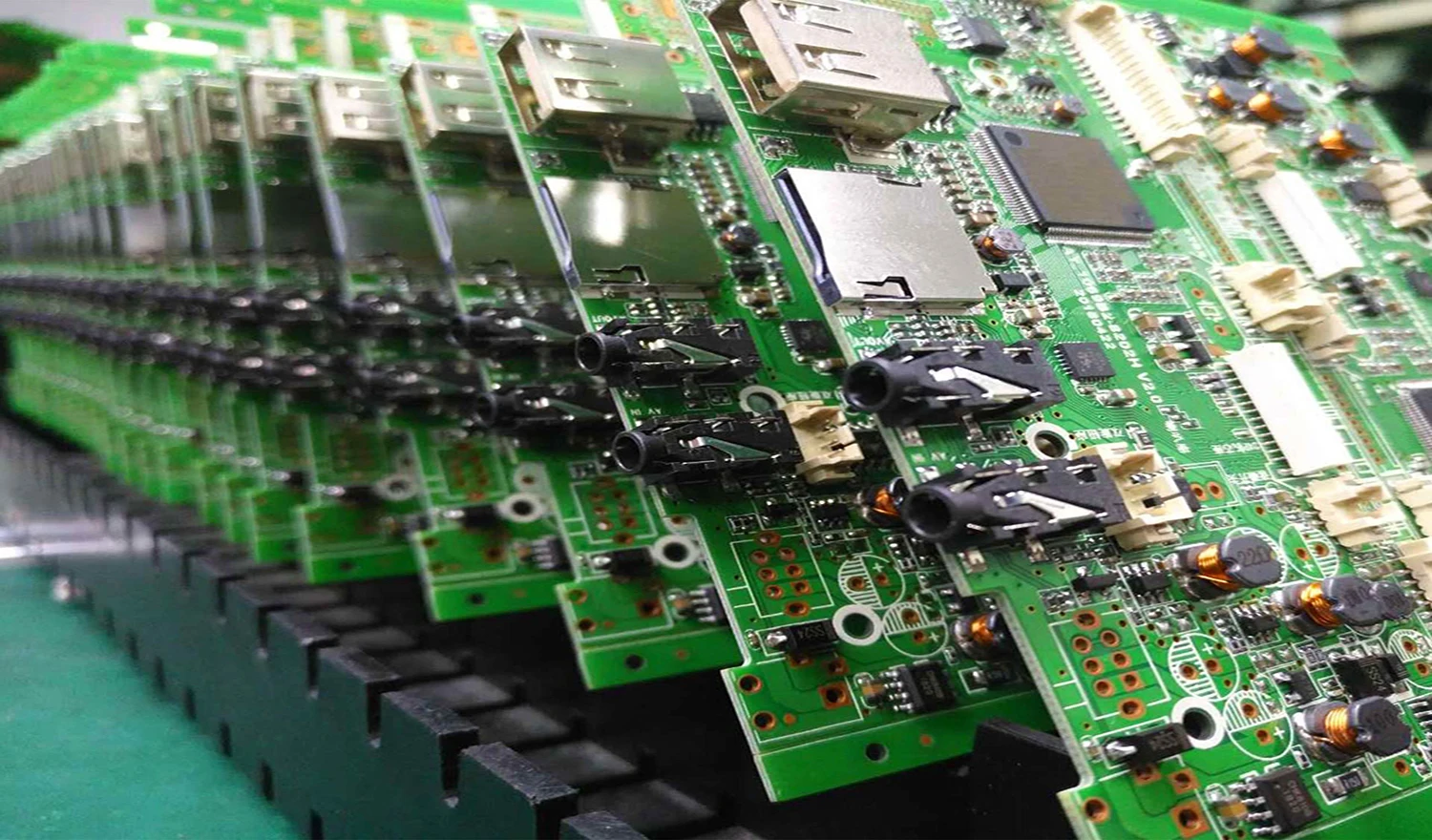
JUKI Pick and Place | PCBA Process

What is a PCB?
PCB=printed circuit board, also known as printed circuit board. It is an important electronic component, a support for electronic components, and a carrier for electrical connection of electronic components. Because it is made by electronic printing, it is called a "printing" circuit board.
What is PCBA?
PCBA=assembly of PCB. Various electronic devices are assembled on the circuit board by a surface encapsulation process. Next is the box assembly, which assembles the assembled PCB with the outer casing to form the finished product. That is to say, the PCB blank board passes through the SMT upper part, and then passes through the entire process of the DIP plug-in, referred to as PCBA. This is a commonly used method in China, and the standard way of writing in Europe and America is PCB'A, which adds a slanting point. PCBA is the PCB with the film attached.
What is the difference between PCB and PCBA?
PCB refers to the circuit board, while PCBA refers to the circuit board plug-in assembly, SMT process.
One is a finished board and the other is a bare board.
PCB (Printed Circuit Board) is called "printed circuit board" and is made of epoxy glass resin material. It is divided into 4, 6 and 8 layers according to the number of signal layers. 4 and 6 layers are the most common. Patch components such as chips are attached to the PCB. PCBA may be understood as a finished circuit board, and PCBA can only be calculated after the process on the circuit board is completed.
PCBA=Printed Cirruit Board +Assembly.
That is to say, the PCB blank board passes through the SMT upper part, and then passes through the entire process of the DIP plug-in, referred to as PCBA.
PCB (Printed Circuie Board) is an abbreviation for printed circuit board. Generally, a conductive pattern formed on a conductive material according to a predetermined design to form a printed circuit, a printed component, or a combination of the two is called a printed circuit. A conductive pattern that provides electrical connection between components on an insulating substrate is referred to as a printed circuit. Thus, the finished board of printed circuit or printed circuit is called a printed circuit board, also known as a printed board or a printed circuit board.
PCBA
The process is a combination of SMT processing and DIP processing. According to the requirements of different production technologies, it can be divided into single-sided SMT mounting process, single-sided DIP cartridge process, single-sided mixing process, single-sided placement and cartridge mixing. Process, double-sided SMT placement process and double-sided mixing process, etc.
PCBA Process Flow Chart Single Side SMT Mounting Single Side DIP Inserting Single Side Mixing Single Side Mounting and Inserting Mixed Double Sided SMT Mounting Double Sided Mixing
Different types of PCB boards have different process processes, and the differences are elaborated below in various cases.
1, single-sided SMT placement
The solder paste is added to the component pad, and after the solder paste of the bare PCB is printed, the relevant electronic components are reflow soldered and then reflow soldered.
2, single-sided DIP cartridge
The PCB board that needs to be plugged in is soldered after the electronic components are inserted into the production line, and the board is cleaned after the welding is fixed. But wave soldering is less efficient
3, single-sided mixing
The PCB board is printed with solder paste, and the electronic components are placed and fixed by reflow soldering. After the quality inspection is completed, DIP is inserted, and then wave soldering or manual soldering is performed. If there are fewer through-hole components, manual soldering is recommended. .
4, single-sided placement and cartridge mixing
Some PCB boards are double-sided, one side is mounted, and the other side is inserted. The process of placement and insertion is the same as that of single-sided processing, but the PCB requires reflow and wave soldering.
5, double-sided SMT placement
In order to ensure the aesthetics and functionality of the PCB, some PCB board design engineers use a double-sided mounting method. Among them, the A side is arranged with IC components, and the B side is mounted with chip components. Make full use of PCB space to minimize PCB area.
6, double-sided mixing
The two methods are mixed in the following two ways. The first method is to assemble the PCBA three times for heating, the efficiency is low, and the pass rate of the wave soldering using the red glue process is low. The second method is suitable for the case where there are many double-sided SMD components and there are few THT components, and manual soldering is recommended. Wave soldering is recommended if there are many THT components.


